Technology of Melfas
We introduce you to MELFAS, a leading touch input solution market company.
Home > Technologies & Products > Technologies
Features and Merits of MELFAS
-
- Rich experiences of the mobile market
- Provision history of more than 700 million Touch Control IC in accumulation to the set enterprise
-
- Holding various Line-up
- Development and Yielding of the IC which can be applied with High-tier & Tablet from Touch Key
-
- Simultaneous supply of Add-on & Oncell·Incell possible which is the only case in Korea
- Success in commercialization of AIT (Advanced In-cell Touch) through the cooperation with LG Display from 3Q 2014
-
- Provision of the optimal Total Solution
- Suggestions of the optimal IC and MELFAS’s own Pattern for the various customers
MELFAS Technologies
-
1) Capacitive Sensing Circuit
Capacitive sensing circuit is the technique which converts the physical capacitance to the electrical signal that can be sensed electrically, and is one of the technologies to design IC which becomes the core of the capacitive sensor. The AC sensing circuit which is being widely used in general measures the responsive signal by the RC time constant which is decided by the R, C components of the electrode after applying the AC signals to the sensing electrode in order to sense the capacitance. In this type of method, since it is affected by R, resistance value among the parasitic components of the sensing electrode, there is a limitation physically not to be able to extract C, capacitance value, only.
To overcome this kind of problem, MELFAS designed the sensing circuit of the inventive fully-analog electric charge. This technology provides certain amount of the electric charge Q to the sensing electrode and charge the electric charge at the both ends of the sensing capacitor C. Thus, the principle is to measure the sensing voltage V which is decided by V=Q/C accordingly.
Through this, C value can be measured regardless of the resistance component of the electrode part, which guarantees the safe performance regardless of the deviation of the resistance value of the electrode part which can rise in the mass production, which enhances the competitiveness of the products from the higher yield and the better product quality. -
2) Design Technology of the ADC Circuit
The ADC circuit which converts the analog signal to the digital data signal is the significant IP which conducts the core function of the sensor. Especially in the sensor that is implemented by the analog circuit, the performance difference of the transistor could rise according to the temperature variation, and the characteristic variation could rise from the user environment and products due to the performance changed by the lot variation.
Our company which holds the temperature correction function which is appropriate for the capacitive sensor application that has unique characteristics and the performance compensation function due to the lot deviation developed and owns the 2-stage ADC structure of the original new temperature compensation.
Through this, MELFAS overcomes the chip performance variation due to the process variation in the mass production, which led to securing the higher production yield and the better product quality. -
3) Low power consumption
To control the mechanical key which was generally used before, MELFAS achieved Wake on GPIO technology, it’s also needed the external interrupt function to sense the input of the mechanical key without any extra current consumption on the sleep mode.
-
4) Design Technology of the Mixed-signal
Touch Screen needs the function part for filtering technology to convert the sensed input information to the coordination information after analyzing it as well as the analog sensing circuit to be immune to the various noises from the external environment.
This kind of functional logic needs to be implemented as the digital circuit, and MELFAS designed this kind of functional logic applying the digital IP with MCU, the memory, etc. Also, it holds the design technology of Mixed-signal to materialize this. -
5) Interface Protocol
Among the Interface I2C UART, SPI slave & master, JTAG, USB2.0 FS/HS, High speed Serial Link, the I2C Interface has the serial communication standard which supports the bi-direction using the smallest number of signal line, and is the universal communication method which the main controller of most cell phones support.
Touch Sensor has to either transmit the input information made by sensing the touch input to the main controller or be transmitted the command packet for the property setting of the touch sensor, and this kind of communication is conducted using the I2C communication standard.
MELFAS designed the Interface circuit and the packet structure which satisfy the I2C standard and holds its own IP. SPI Interface(Slave/Master) supports the fastest transmission speed in the low price type of Interface and is possible to the 1(Master):N(Slave) communication as the synchronous method, but it is 1:1 communication once Slave is selected by the Master. MELFAS has both the Master/Slave IP designed by itself. JTAG Interface is the Interface which can simply test in IC instead of MCU. MELFAS has JTAG IP as well.
USB 2.0 Interface can give and take the data with the fastest transmission speed. Another, High speed Serial Link is the Interface which sends the image which was received at the MIPI to the Driver IC. -
6) Analog Filter
As the block which belongs to Touch AFE (=analog front end), it was designed to adjust the filter bandwidth in order to minimize the amount of the noise and avoid the certain noise after sensing.
-
7) Digital Filter
MELFAS has the various digital filter algorithms to remove the quantization-noise (digital noise) and a certain or the residual noise after minimizing the noise at the analog path and passing through ADC.
-
8) Voltage Regulator Technology
Due to the features of the analog sensing circuit, the abnormal operation could occur from the abrupt power supply change caused by the power supply noise.
In order to prevent the deterioration of the circuit performance due to the power supply change like this, the external voltage regulator is normally needed. However, MELFAS integrated this IP into the chip and secured the stable sensor performance without any cost increase. -
9) SoC Technology
To implement the effective digital control circuit based on MCU + Non-volatile memory (NVM) integrated system, instead of the hard-wired control circuit which was applied in the 1st-generation sensor, MCU IP was applied from the 2nd-generation sensor. The integrated MCUs are used from 8-bit 8051 type of MCU core IP widely provided to 32bit ARM MCU core IP. This includes memory interface, ROM control, ISP (In System Programming), GPIO control, peripheral control.
-
10) Peripheral IP
Timer, Watchdog, GPIO, PWM, Timer are operated to periodically inform the Interrupt to MCU through the internal counter, and Watchdog, which is similar to the Timer, has the function to reset the system in case the Interrupt which was delivered to MCU is not processed properly. Also, GPIO can support the various interfaces with the external devices, and it helps to improve the performance of the low power consumption through PWM.
-
11) Design technology of ESD protection circuit
Unlike the ordinary sensor, the capacitive touch sensor is generally located at the nearest to the set case outskirt due to the characteristics of an input device. In accordance with this, it is difficult to meet in the set condition only with general ESD protection circuit of HBM 2KV of IEC61000-4 standard which is required at the general commercialized chip. To overcome this, MELFAS has not used the general ESD protection circuit which is included in the standard I/O from the foundry, but developed its own ESD protection circuit based on it. Through this, the competitiveness has been secured having the ESD protection circuit performance of the HBM 6KV which is superior to other competitors.
-
12) Hover Technology
MELFAS has the technical patent to be possible to detect the fine cap changes, and this technology was applied to the fingerprint sensor and the high-end mobile/tablet.
-
13) The Capture technology of 500dpi level image
With the use of the MELFAS Hover related technical patent, the detection of the fine level of cap changes became possible, which enabled to capture the image with 500dpi level that is required at the popular fingerprint specification. Also, the algorithm for the security was additionally implemented.
-
14) Firmware (with proprietary)
-
- Frequency Hopping :
- In the environment with the various type of the noise, it finds the frequency range of the noise-free and avoid any malfunction.
-
- Precise Hover Rejection :
- Being recognized with the input without the finger’s touching the screen impacts the users’ feeling of the performance very badly. We solved this by exactly calculating the input area of the recognized input and applying differently with the area.
-
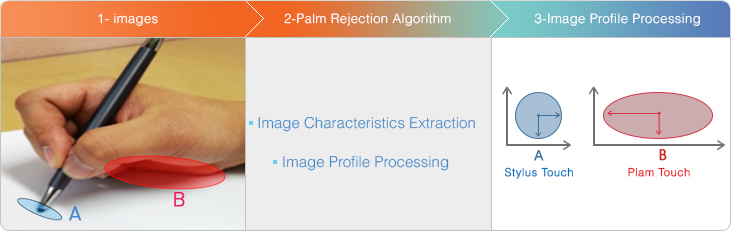
- Palm Rejection :
- In case the stylus of the contact area under 2.5phi is used, the user can put his/her hands on, or use the pen holding the touch screen with the other hand. At this moment, the algorithm can inform AP of whether each finger is the part of the palm touch or not in order to be recognized only stylus input.
-
- Finger Separation :
- The 2 touches which were contacted closely are exactly recognized 2 of them by checking the form of the image when applying the multi touching.
-
- Gesture Detection :
- Recognition of the letters (characters) such as c, w, v, m, s, z, o, e, etc as well as the action of the double tap and left/right/up/down flick.
-
- Dynamic Position Filter :
- According to the input speed and the direction of the user, the coordination stabilized logic is operated with the optimum. The linearity of the input is secured without any delay phenomenon of the coordination through this.
-
- Signature Detection :
- As a method to compare to the signature information which was put in advance and to match them, it is a lock lift solution with the higher security.
-